An Overview of RF Circuit Simulation
![]() Back to RF.Spice A/D Wiki Gateway
Back to RF.Spice A/D Wiki Gateway
Contents
- 1 Understanding RF Circuit Analysis as an Analog Simulation
- 2 RF Circuit Simulation vs. Electromagnetic Simulation
- 3 Multiport Networks
- 4 List of Standard Imported RF Devices
- 5 Generic Transmission Lines
- 6 Physical Transmission Lines
- 7 List of Physical Transmission Line Types
- 8 Working with Coupled Transmission Line Devices
Understanding RF Circuit Analysis as an Analog Simulation
You can use RF.Spice A/D to simulate or design distributed analog and mixed-mode circuits at high frequencies. RF circuit analysis, by nature, is an AC analysis that you typically run at high frequencies ranging from tens of Megahertz to tens of Gigahertz. At such high frequencies, the dimensions of your circuit may become comparable in order of magnitude to the wavelength, when wave retardation effects start to appear. In other words, your circuit starts to act like a distributed structure rather than a lumped circuit where signals propagate instantaneously. In the analysis of a low frequency circuit, two nodes that are connected to each other through a wire are assumed to have equal potentials or identical voltages. In RF circuits, however, parts and devices are connected to one another using transmission line segments, which introduce additional phase shifts depending on their electrical lengths and may also alter the voltages and currents at different points of the circuit due to impedance mismatch.
RF.Spice A/D uses the same Berkeley SPICE and XSPICE simulation engines of its forerunner B2.Spice A/D. In other words, the high frequency AC analysis is carried out by the same analog and mixed-mode SPICE simulation engines based on nodal admittance analysis, which have been enhanced with additional RF simulation capabilities. As a result, you can mix the RF devices in your circuits with all the other analog and mixed-mode devices. You can also mix transmission-line-type RF devices with digital parts and perform mixed-mode time domain simulations.
The concepts of transmission lines and multiport networks are integral to any RF simulation. From a simulation point of view, an RF circuit is made up of a collection of multiport networks that are interconnected via transmission lines segments or components. If the input of your circuit is connected to a source and its output is connected to a load, then you can compute all the voltages and currents at all various circuit nodes, some of which may serve as external or internal ports of your circuit. Or you can calculate the port characteristics of the overall network by designating input and output ports to your RF circuit.
All the RF devices of RF.Spice A/D can be divided into two groups: devices based on transmission line models, and devices based on multiple networks. RF.Spice's transmission line models are enhanced versions of SPICE's standard LTRA model. The transmission-line-based devices typically utilize a combination of LTRA and passive RLC models. Multiport networks are characterized and modeled based on their frequency-domain scattering (S) parameters. The S-parameters are tabulated as a function of frequency, and their values are interpolated in between the frequency samples. RF.Spice A/D performs an AC analysis of these RF devices by converting their S-parameters to Y-parameters and using them in conjunction with SPICE’s nodal admittance matrix formalism. The S-parameter-based RF devices of RF.Spice A/D are primarily intended for use in two types of tests:
- AC Frequency Sweep Test
- Network Analysis Test
![]() RF.Spice A/D RF Tutorial Lessons Gateway
RF.Spice A/D RF Tutorial Lessons Gateway
| |
S-parameter-based RF devices do not work with “Live Simulation” or Transient Test as their models typically contain S-parameters at high frequencies only. |
RF Circuit Simulation vs. Electromagnetic Simulation
The RF circuit analysis performed by RF.Spice A/D is based on the assumption that your distributed RF circuit can be modeled as an interconnected network of multiport devices and transmission line segments and components. This means that all the coupling or crosstalk effects must have been captured by the S-parameter-based models of devices or by the transmission line and discontinuity models used by RF.Spice A/D. Most of these models work satisfactorily at lower frequencies up to several Gigahertz. At these frequencies, a quasi-static regime may be able to represent the physics of your RF circuit to a good level of accuracy. In the quasi-static regime, the different parts of your circuits can be treated as multiport devices or components that are governed by the Kirchhoff circuit laws.
As the frequency increases, more complex wave radiation and propagation effects start to appear and affect the performance of your circuit. At much higher frequencies and in the millimeter wave region of the spectrum, the coupling between adjacent transmission lines may no longer be neglected. In such cases, a full-wave electromagnetic analysis of portions of the circuit might become inevitable. This might be especially true for junction areas and vertical interconnects that join transmission line traces on two sides of a board and across different substrate layers. For accurate analysis of structures of this type you need a full-wave electromagnetic (EM) modeling tool. EM.Cube is a modular suite of EM simulation tools for this very purpose. Among its computational modules are time domain full-wave simulators like EM.Tempo based on the Finite Different Time Domain (FDTD) method as well as frequency domain full-wave simulators like EM.Picasso and EM.Libera based on different variations of the Method of Moments (MoM).
| |
You can analyze a complex passive multiport device in EM.Cube and import its simulated S-parameter data into RF.Spice A/D as a new custom device in your parts database. |
Multiport Networks
A multiport network is a frequency-domain “black-box” block that is modeled by its S-parameters as a function of frequency. RF.Spice A/D currently offers the following models:
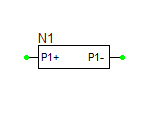
- Complex Impedance (a two-pin device)
- One-port (a two-pin device)
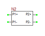
- Two-port (a four-pin device)
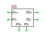
- Three-port (a six-pin device)
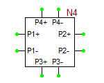
- Four-port (an eight-pin device)
Each pair of pins form a port of the device. In other words, an N-port device has 2N pins or terminals. In most cases, the negative pin of a port is grounded, while its positive pin is connected to the other parts of your circuit. It is very important that all the pins of a multiport device are properly connected to ensure a successful simulation.
An N-port device is characterized by a complex-valued NxN scattering (S) matrix. A one-port has only one S-parameter, i.e. s11. A two-port has four S-parameters: s11, s21, s12 and s22. A Complex Impedance is a special type of one-port that is defined by its complex-valued z11 parameter rather than by s11. Multiport networks can be connected to one another through their ports. For example, you can cascade two two-ports as shown in the opposite figure. Note how the negative pins of the two devices have been grounded.
| |
Multipart Network devices do not work with “Live Simulation” or Transient Test as their models normally contain S-parameters at high frequencies only. |
Defining S-Parameters
Each multiport network device has a property dialog where you can specify its S-parameters as a function of frequency. Each row of the S-parameter table in the property dialog represents a frequency sample. The complex-valued elements of the scattering matrix are listed column by column in each row of the table after the frequency value. For example, for a two-port, the format is as follows:
Freq Real(s11) Imag(s11) Real(s21) Imag(s21) Real(s12) Imag(s12) Real(s22) Imag(s22)
You need to specify the frequency units, which is Hz by default. You also need to specify the format of the complex numbers. There are three options:
- Real / Imaginary
- Magnitude /Phase
- dB / Phase
Phase is always specified in degrees. For most passive devices, you normally use a Re/Im format. However, the manufacturer data sheets of active devices like BJTs, MOSFETs and MESFETs typically specify the S-parameters in dB/Ph format with the frequency expressed in GHz.
Among RF.Spice's multiport network device, the one-port, two-port, three-port and four-port are all defined based on their S-parameters. All multiport network devices have a "Port Reference Impedance" parameter. The default value of the reference impedance is 50 Ohms for the one-port, two-port, three-port and four-port. For most RF circuits, you do not have to touch the 50Ω default value.
Besides entering the S-parameter values manually using in the parameter table, you can directly import these values from a text file with a ".TXT" file extension. For this purpose, click the button labeled "Load from File..." in the property dialog. This opens up the standard Windows Open dialog, with the file type set to text files. Browse your folders and select the text file to load the data from. The S-parameters you import to RF.Spice A/D can come from manufacturer data sheets or they can be generated by electromagnetic simulation suites such as EM.Cube. For example, among EM.Cube's computational modules, the FDTD, Planar MoM, Wire MoM and Surface MoM simulation engines all generate S-parameter text files for structures with port definitions. These files can directly be loaded into RF.Spice A/D.
The Complex Impedance Device
In many RF circuit problems, you may need to define a fixed impedance element, e.g. as a load. Complex Impedance is a special one-port network device that is defined based on its z11 parameter. Therefore, the format of the parameter table for Complex Impedance is:
Freq Real(z11) Imag(z11)
Note that the default reference impedance of the Complex Impedance is zero and must always stay zero to function properly. In order to have a fixed impedance element, define the same Real(z11) and Imag(z11) values for the minimum and maximum frequencies of your circuit. Due to the interpolation between these two values, you will always get the same impedance value at all the frequencies in between those two limits.
List of Standard Imported RF Devices
Generic Transmission Lines
The standard SPICE provides two types of general-purpose transmission line models: lossless (TRA) and lossy (LTRA). These models are primarily intended for transient analysis. The lossless transmission line model is characterized by either its delay in seconds or by its normalized length at a given frequency. On the other hand, the lossy transmission line model is characterized by distributed RLCG parameters: resistance per unit length (R), inductance per unit length (L), capacitance per unit length (C), and conductance per unit length (G). Both B2.Spice A/D and RF.Spice A/D offer the native SPICE transmission line models TRA and LTRA as passive devices.
However, RF.Spice A/D also offers a number of other transmission line models specifically intended for use in RF circuit analysis. These include the generic T-Line, the generic coupled T-lines, and a variety of physical transmission line models.
The Generic T-Line
RF.Spice A/D offers a passive device called Generic T-line with the keyboard shortcut “T”, which is a general purpose frequency-domain transmission line segment model. It is based on the native SPICE LTRA model, but with the following parameters:
- Z0: Characteristic Impedance in Ohms
- eeff: Effective Permittivity
- alpha: Attenuation Constant in dB/m
- len: Physical Length in meters
The default parameters of the Generic T-Line are Z0 = 50 Ohms, eeff = 1, alpha = 0, and len = 10mm. A unit effective permittivity implies a TEM transmission line because √εeff = β / k0, where β is the propagation constant of the transmission line and k0 = 2πf/c is the free space propagation constant, with f being the frequency in Hertz and c = 3e8 m/s being the speed of light. A zero attenuation constant represents a lossless transmission line. The Generic T-Line device is indeed a two-port network with a 2×2 scattering matrix or four S-parameters: s11, s21, s12 and s22. Obviously, this is a reciprocal and symmetric network, i.e., s11 = s22, and s21 = s12.
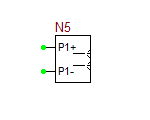
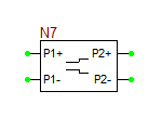
Note that N-port networks in RF.Spice A/D have schematic symbols with 2N pins. Each pair of pins represents a port. In a similar way, the generic T-line has two ports and four pins. The pins are marked with plus and minus signs. For example, in the figure above, the pins P1+ and P1- together form Port 1. Normally, the negative pins are grounded, and the positive pins are connected to the other parts of the circuit.
| |
Proper grounding of the transmission line devices is critical for a successful simulation. |
Open and Short Stubs
The Generic Open Stub and Generic Short Stub are two one-port devices based on the Generic T-Line device. They represent terminated generic transmission line segments. In the open stub case, the termination load is ZL → ∞, and in the short stub case, the termination load is ZL = 0. The parameters of both open and short stub devices are the same as those of the generic T-line device.
Generic T-Line Discontinuities
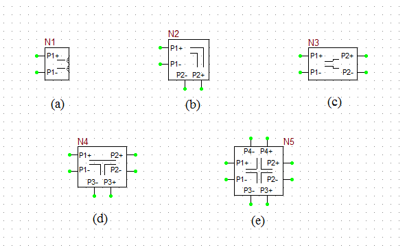
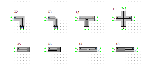
In real practical RF circuits, you often need to transition from one transmission line to another or connect two or more transmission lines together. These transitions can be modeled as multiport networks. RF.Spice A/D currently offers five generic T-Line discontinuity devices as follows:
- Generic Open End (a one-port)
- Generic Bend (a two-port)
- Generic Step Junction (a two-port)
- Generic Tee Junction (a three-port)
- Generic Cross Junction (a four-port)
The schematic symbols of these devices are shown in the opposite figure. Similar to other RF devices or multiport networks, the negative pins of the ports must always be grounded. Unlike the T-line device described earlier which have models based on or derived from the standard SPICE LTRA, the generic T-line discontinuities have S-parameter-based models.
When you first place these discontinuity parts on your circuit, they have default S-parameter values. The default values have been chosen to be very general and may not necessarily represent the physics of your specific circuit. You must enter your own S-parameter values over the desired frequency range and replace the default values. These data can easily be generated in and imported from an electromagnetic simulation suite like EM.Cube. Unlike physical transmission lines like microstrip or coaxial line (to be discussed later) that have particular geometries and physical structures, the Generic T-Line device and Generic T-Line Discontinuities are very general by definition and do not have physical, material or dimensional parameters. You can model and simulate very complicated transmission line structures as well as open end, bend, step, tee or cross junctions based on those structures using EM.Cube and then import their S-parameter data into the corresponding discontinuity parts.
For more information about generic transmission line discontinuity devices, please refer to Glossary of Generic RF Devices.
Physical Transmission Lines
The Variety of Physical Transmission Line Types
In addition to the Generic T-Line, RF.Spice A/D also offers a large number of physical transmission lines as follows:
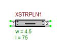
- Microstrip Line
- Coupled Microstrips
- Covered Microstrip
- Suspended Microstrip
- Inverted Microstrip
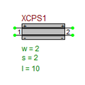
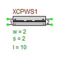
- Coplanar Strips (CPS)
- Stripline
- Coupled Striplines
- Off-Center Stripline
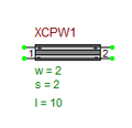
- Coplanar Waveguide (CPW) Line
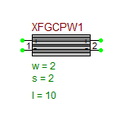
- Finite-Ground CPW Line
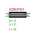
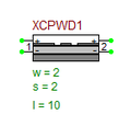
- Conductor-Backed CPW Line
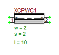
- Covered CPW
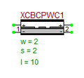
- Covered Conductor-Backed CPW
- CPW with a Superstrate
- Double-Layer CPW
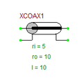
- Coaxial Line
- Twin-Lead Line
- Twisted-Pair Line
The physical transmission line types are characterized by their physical dimensions and material properties.
Physical Line Calculators and Designers
When you place a generic T-line part in your circuit, you have to specify its characteristic impedance (Z0), effective permittivity (eeff) and attenuation constant (alpha). In the case of physical transmission line parts like mircostrip, coaxial line or CPW, you specify the physical parameters of the line such as various dimensions and material properties. RF.Spice A/D then automatically calculates the necessary transmission line parameters at the time of simulation based on your physical data.
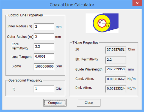
For every physical transmission line type listed above, the Device Manager of RF.Spice A/D provides a corresponding Line Calculator. The line calculators are accessible form the Tools Menu of the Device Manager. The line calculators take the substrate properties and the physical dimensions of a line types and calculate its characteristic impedance (Z0) and effective permittivity (eeff). The Line Calculator dialog also has an "Operational Frequency" input with a default frequency of 1GHz, which is used to calculate the guide wavelength of the transmission line at that frequency. In many practical applications, you need quarter-wavelength line segments. In that case, you must first calculate the guide wavelength of the transmission line as defined by λg = λ0 / √εeff, where λ0 = c/f is the free space wavelength at the operational frequency.
Some of physical line types such as microstrip, stripline, coaxial line, twin-lead line and twisted-pair line, have loss parameters: dielectric loss tangent and metal conductivity. For these lines, the line calculator calculates the conductor attenuation constant (αc) and dielectric attenuation constant (αd), both in Neper per meter (Np/m). Note that the total attenuation constant is the sum of these two: α = αc + αd. You can convert the value of attenuation constant from Np/m to dB/m using the relationship 1Np = 8.6859dB.
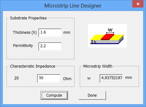
You often need to design a 50Ω transmission line of a certain type. RF.Spice A/D provides ten physical transmission line design tools for:
- Microstrip Line
- Coupled Microstrips
- Stripline
- Coupled Striplines
- Coplanar Waveguide (CPW) Line
- Finite-Ground CPW Line
- Conductor-Backed CPW Line
- Coaxial Line
- Twin-Lead Line
- Twisted-Pair Line
The above line designers ignore the conductor and dielectric losses and calculate the physical dimensions of the line for a given value of the characteristic impedance Z0. For example, given a substrate with thickness h and relative permittivity εr, the "Microstrip Designer" calculates the microstrip width in mm for a given value of Z0 (50 Ohms by default). Some line type like CPW and coaxial line have more than one dimensional parameter that can be varied. For example, CPW has slot width (w) and center strip width (s), while coaxial line has inner and outer conductor radii. In such cases, the line designer dialog provides radio button options to fix one parameter and vary the other.
Physical Transmission Line Discontinuities
Besides the Generic T-Line Discontinuity devices described earlier, RF.Spice A/D also offers a large number of physical transmission line discontinuity devices based on some of the transmission line types listed above. Among these, the microstrip components are more widely used and have more variety. Unlike the generic T-line components which require that you supply the S-parameter data, the physical components are parameterized based on their geometrical and material properties. As a result, you simply enter the physical dimensions and other parameters and their S-parameters are automatically calculated by RF.Spice A/D during the circuit simulation. In other words, the property dialog of these components contains their physical parameters only and does not show the values of their S-parameters as a function of frequency.
![]() For more information about physical transmission line discontinuity devices, please refer to Glossary of Physical Transmission Lines and Components.
For more information about physical transmission line discontinuity devices, please refer to Glossary of Physical Transmission Lines and Components.
List of Physical Transmission Line Types
Working with Coupled Transmission Line Devices
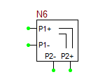
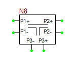
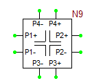
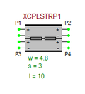
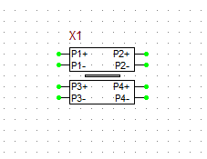
Many passive RF devices such as directional couplers, hybrids and some filter designs involve segments of parallel coupled transmission lines. According to the coupled mode theory, one can define even and odd mode impedances (Z0e and Z0o) for such transmission lines. The resulting RF structure can be modeled as a four-port network device as shown in the opposite figure. Note that the four-port device has eight pins. Ports 1 and 2 correspond to the input and output of the first transmission line segment, while Ports 3 and 4 correspond to the input and output of the second (coupled) line segment. It is very important to connect and ground the negative pins at the input and output of the two transmission line segments.
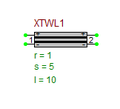
RF.Spice A/D provides three coupled line devices, all of which assumes lossless transmission lines:
- Generic Coupled T-Lines
- Coupled Microstrips
- Coupled Striplines
The Generic Coupled T-Lines device has the following parameters:
- Z0e: Even Mode Characteristic Impedance in Ohms
- Z0o: Odd Mode Characteristic Impedance in Ohms
- eeff: Effective Permittivity
- len: Physical Length in meters
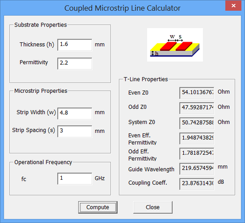
The coupled microstrips and coupled stripline devices are characterized by their strip width, strip spacing and substrate properties. The Coupled Microstrips Calculator and Coupled Striplines Calculator find the even and odd mode impedances for the given strip width and strip spacing. They also calculate the even and odd mode effective permittivities, which are typically different. The system characteristic impedance of the coupled line is calculated from the formula:
- [math] Z_0 = \sqrt{ Z_{0e} . Z_{0o} } [/math]
To calculate the guide wavelength, the average of the two effective permittivities is used. In addition, the coupling coefficient of the coupled line is calculated in dB from the formula:
- [math] C = \frac{ Z_{0e} - Z_{0o} }{ Z_{0e} + Z_{0o} } [/math]
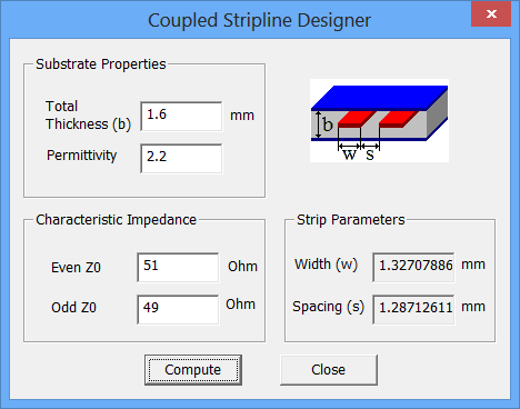
The Coupled Microstrips Designer and Coupled Striplines Designer, on the other hand, find the values of the strip width and strip spacing for given values of the even and odd mode characteristic impedances.
